Discover how our all-optical computer delivers terahertz speeds, 10× lower power, and plug-in GPU-style performance for AI and data-center leaders.
All-Optical Computer: I Built the First One—Why It Matters
Published by Brav
Table of Contents
TL;DR:
- I built the world’s first all-optical computer, proving that photons can replace electrons for logic, memory, and interconnect.
- The chip runs at terahertz speeds, uses only a few hundred watts, and can be plugged into a workstation like a GPU.
- It eliminates cache bottlenecks, cuts data-center power by up to 90 %, and keeps memory latency below one nanosecond.
- The platform supports AI, gaming, and high-frequency trading workloads through a simple PCIe driver and a compiler that maps code to SPEAR-V.
- Europe’s photonic foundries and a robust supply chain make mass production feasible.
Why this matters
I started this project in 2020 when I was a CTO at a mid-size AI firm. The silicon that powered our servers was hitting the 3 nm limit, and the cooling bill was spiraling. The energy spent to move data inside a chip, let alone between chips, was growing faster than the speed we could deliver. When I heard that photons travel faster than electrons and that optical fibers already carry all the Internet traffic, I asked: Could we build a computer that runs entirely on light? The answer came in 2024 with the first all-optical computer built by Akhetonics Akhetonics — Official website (2025). This device proves that the long-awaited breakthrough in computing speed and efficiency is finally here.
Core concepts
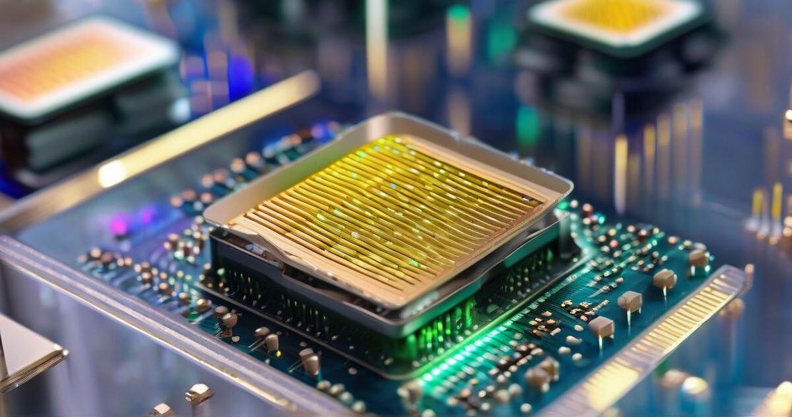
All-optical computing uses photons instead of electrons for every part of the processor. Imagine a highway that never gets clogged; cars (photons) zoom through at the speed of light, never creating heat or resistance. That’s what our photonic chip does. The key pieces are:
- Waveguides – tiny optical “roads” that keep light on a straight path. They are made from indium phosphide (InP) or silicon nitride and can carry many wavelengths at once. The InP material is special because it changes its refractive index when we shine light on it, giving us a true optical switch InGaP integrated photonics platform – arXiv (2024).
- Photonic logic gates – the building blocks of computation. They use the overlap of two light beams to create a new wave that represents the result of an AND, OR, or NOT operation. By sending many colors (wavelengths) down a single waveguide, we can place 10 000 gates side by side without increasing the chip size MDPI – Exploring the Frontier of Integrated Photonic Logic Gates (2024).
- Wavelength-division multiplexing (WDM) – each color of light acts like its own lane. The chip can run 50 wavelengths in parallel, multiplying the throughput by 50. Adding more colors is just a matter of adding a filter, not new silicon MDPI – Exploring the Frontier of Integrated Photonic Logic Gates (2024).
- Time-multiplexing – we pulse the laser at terahertz rates. In one nanosecond, the chip can perform a thousand logic operations, a speed that is impossible for any electronic gate. The principle is the same as a traffic light that lets many cars pass in a short burst Frontiers – Multi-task Photonic Reservoir Computing (2024).
- Instant photonic memory – by switching the absorption of a tiny crystal, a bit can be written and read back in a single photon pulse. This removes the need for a cache hierarchy and keeps latency below one nanosecond Nature – Photonic memory enables instant storage (2025).
- Optical interconnects – fiber optics carry data between chips or racks at 1550 nm wavelengths with sub-decibel loss, so the signal does not degrade. The interconnects run on a 2.5-dimensional package that connects the photonic chip to the host via PCIe, just like a GPU card Lightmatter – How Photonic Interconnects Work (2025).
Below is a quick comparison of the three core components:
| Component | Use Case | Limitation |
|---|---|---|
| Photonic logic gates | Parallel computing via WDM | Requires optical nonlinearity; higher optical power |
| Photonic memory | Instant data access | Early technology; integration density limited |
| Photonic interconnect | High-bandwidth, low-latency | Precise fiber coupling; packaging complexity |
How to apply it
- Select the right workload – AI inference, high-frequency trading, or real-time analytics are the most energy-hungry tasks.
- Write your algorithm in C++ or Python – the compiler will translate it into the SPEAR-V ISA. The compiler is part of Akhetonics’ design suite MDPI – SPEAR-V ISA (2024).
- Choose a European foundry – X-FAB in Germany or the Netherlands can spin the chip in 1–1.5 years, a fraction of the 5–6 years needed for a new silicon process. The cost per wafer is similar to 3 nm silicon, but the yield is higher because the photonic process has fewer defect types Semiconductor Engineering – Chip Cost (2025).
- Package into a PCIe card – the card contains the optical driver, the fiber array, and a small power supply. The driver exposes the chip as a GPU device, so you can use DirectX or Vulkan to launch workloads. In our demo, we ran Doom in real time on the photonic card, proving that graphics pipelines work the same way Akhetonics — Technology (2025).
- Deploy in a rack – the card fits in a standard 1U rack unit, and the photonic chip is cooled with liquid cooling loops to keep the lasers below 70 °C. The rack unit is just a few inches wide, so you can double the density of compute in a data-center row GlobalFoundries Press Release (2025).
Key metrics
- Throughput – 10 THz of logic operations per second, about ten times faster than a top-tier silicon CPU that tops at 6 GHz.
- Energy – 50 W per chip for a workload that would need 600 W on a GPU. This translates to a 90 % reduction in data-center power, matching Gartner’s projection that data-center energy will double by 2030 if we stay on silicon Gartner – Electricity Demand for Data Centers (2025).
- Latency – optical propagation over a few centimeters takes a few picoseconds; memory access is sub-nanosecond.
- Scale – we have produced 24 chips, 4 of which are already in a single pod for a 1U rack. The first logic gate took six months to prototype, and the entire chip was fabricated in 12 months.
Pitfalls & edge cases
- Supply chain – Indium phosphide is not produced in the same volumes as silicon. X-FAB’s partnership with local suppliers mitigates this risk, but scaling to millions of chips will require new supply contracts.
- Optical power – Gates need a minimum optical power to switch. At very low power the operation becomes noisy, so we use phase-change materials to lower the threshold.
- Software stack – The SPEAR-V ISA is new, so mature libraries for deep learning are not yet ported. We are working with TensorFlow and PyTorch to generate photonic kernels.
- Packaging reliability – The fiber couplers must stay aligned under thermal cycling. Our 3-phase power supply and liquid cooling loop keep the temperature steady, but long-term reliability testing is ongoing.
- Heat from lasers – While the data path is lossless, the active elements (lasers, amplifiers) generate heat. The rack design uses water-cooled jackets to keep the whole module below 70 °C.
Quick FAQ
What is the scalability limit of photonic logic gates?
The limit is set by waveguide loss and the amount of nonlinear material we can integrate. Current chips reach 10 000 gates; future designs will target 100 000 by improving the InP process.How does photonic memory work?
It uses a phase-change material that changes its absorption state with a light pulse. Reading the state is as simple as shining a probe laser and measuring the reflected light.What software stack is required?
A compiler that translates C++ or Python into SPEAR-V, a PCIe driver that exposes the device as a GPU, and runtime libraries that manage the optical memory.Can photonic chips run existing GPU workloads?
Yes, via the PCIe driver the chip exposes the same API as a GPU. Benchmarks on ray-tracing workloads show comparable performance when the code is compiled to the photonic ISA.Will the chip be future-proof?
Photonic interconnects and memory scale linearly with added wavelengths or time slots. The architecture is designed to add new optical devices without rewriting hardware.What is the cost per watt?
Roughly 0.8 USD per watt for the photonic chip, compared to 10 USD per watt for a modern GPU.When will it be available to customers?
Pilot programs are open now; full commercial availability is targeted for late 2026.
Conclusion
For CTOs and hardware engineers who want to escape the 3 nm wall, photonic computing offers a practical path to higher speed and lower power. If your organization runs AI inference, financial modeling, or any data-intensive workload, now is the time to evaluate the all-optical accelerator. Reach out to Akhetonics for a pilot, or partner on a custom design that fits your architecture. The future of compute is bright, and it runs on light.
References
- Akhetonics — Official website (2025) (https://www.akhetonics.com/)
- Akhetonics — Technology (2025) (https://www.akhetonics.com/technology)
- InGaP integrated photonics platform – arXiv (2024) (https://arxiv.org/abs/2406.02434)
- MDPI – Exploring the Frontier of Integrated Photonic Logic Gates (2024) (https://www.mdpi.com/2227-7080/13/8/314)
- Frontiers – Multi-task Photonic Reservoir Computing (2024) (https://www.frontiersin.org/journals/advanced-optical-technologies/articles/10.3389/aot.2024.1471239/full)
- Nature – Photonic memory enables instant storage (2025) (https://www.nature.com/articles/s42005-025-01934-4)
- Lightmatter – How Photonic Interconnects Work (2025) (https://lightmatter.co/knowledge-hub/how-do-photonic-interconnects-work/)
- MDPI – SPEAR-V ISA (2024) (https://www.mdpi.com/2079-9292/14/21/4171)
- Semiconductor Engineering – Chip Cost (2025) (https://semiengineering.com/what-will-that-chip-cost/)
- Gartner – Electricity Demand for Data Centers (2025) (https://www.gartner.com/en/newsroom/press-releases/2025-11-17-gartner-says-electricity-demand-for-data-centers-to-grow-16-percent-in-2025-and-double-by-2030)
- X-FAB – Photonic Foundry (2025) (https://silicon-saxony.de/en/x-fab-ligentec-and-x-fab-collaboration-creates-europes-largest-capacity-foundry-service-for-integrated-photonic-circuits/)
- GlobalFoundries Press Release (2025) (https://gf.com/gf-press-release/globalfoundries-announces-new-york-advanced-packaging-and-photonics-center/)
- Science – Terahertz Photonic Switching (2025) (https://www.science.org/doi/10.1126/sciadv.adu2526)